
What is a Gunn Diode? It’s Symbol, Construction, Working, Advantages Disadvantages and Applications
A diode is a semiconductor-based component that allows current in only one direction. It has two terminals anode and cathode. It is an electronic switch that has very low resistance in forward bias and very high resistance in reverse bias. It is used for rectification and switching signals.
There are several types of diodes designed to perform specific functions. Gunn diode is one of the types of food diodes used for its negative resistance characters and very high switching speed in microwave frequency. This article explains Gunn diode in detail.
Gunn Diode
A Gunn diode is a type of diode having two terminals with negative resistance used for its very high switching speed. Though it is not considered a diode since it does not contain a conventional PN junction but is made of a single N-type semiconductor. It is why it is known as a Transfer Electron Device “TED“. It can conduct in both directions, therefore it can’t be used for rectification. It is termed a diode because it has two terminals anode and cathode.
It works on the principle of ‘Gunn effect’. The phenomenon is named after British physicist John Battiscombe Gunn (J.B. Gunn) who discovered it in 1963. He observed that after applying very high voltage to a very thin layer of semiconductor, high-frequency oscillations are generated.
It is usually made of gallium arsenide GaAs whose operating frequency reaches up to 200 GHz and gallium nitride GaN, Gunn diode’s operating frequency reaches up to 3 THz.
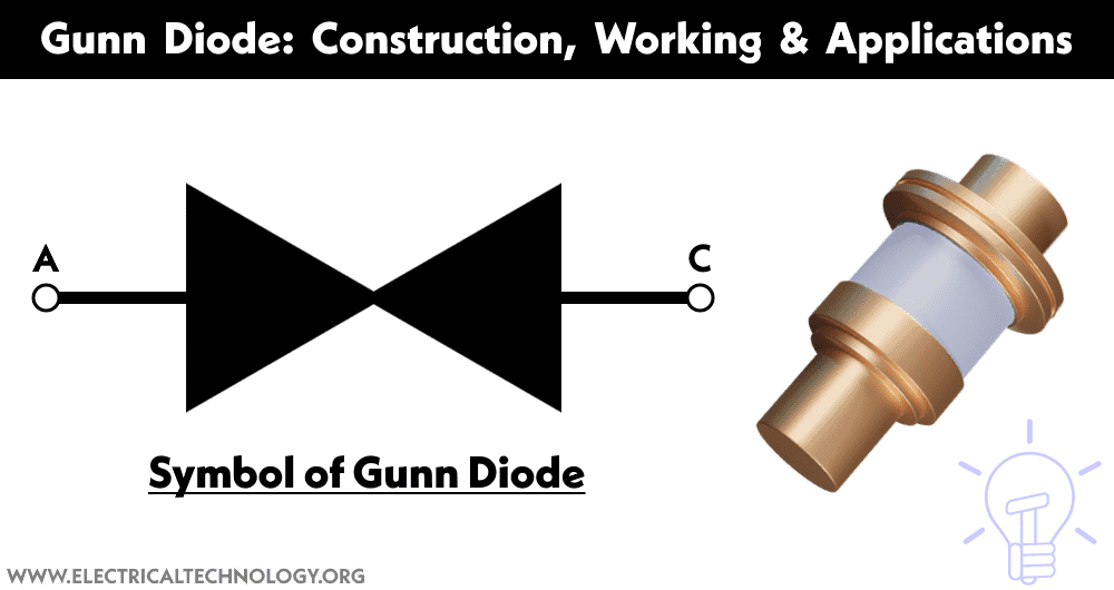
Symbol of Gunn Diode
The symbol of the Gunn diode resembles two conventional diodes connected face to face as shown in the figure below.

Related Posts:
- What is Diode? Construction and Working of PN Junction Diode
- Types of Diodes and Their Applications – 24 Types of Diodes
Construction
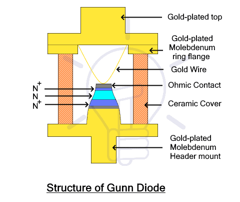
The Gunn diode is made of only an N-type semiconductor because the transferred electron effect (explained below) only occurs in N-type materials and it does not occur in P-type materials because it is only appropriate for electrons and not holes. The materials used for Gunn diode are Gallium Arsenide (GaAs), Gallium Nitride (GaN), Indium Phosphide (InP), Indium Arsenide (InAs), Indium Antimonide (InSb), Cadmium Telluride (CdTe), Cadmium Sulphide (CdS) and Zinc Selenide (ZnSe). All these materials have electrons as majority carriers.

Gunn diode is made of actually three layers of N-type material. The two layers at the extremes are heavily doped while the middle thin layer is lightly doped known as the buffer layer. Generally, the middle thin layer is epitaxially grown on the N+ substrate. While the topmost layer N+ layer is formed by the ion implantation technique. Thus forming three layers semiconductor structure. The width of the middle layer determines the operating frequency of the device. Metallic or ohmic contacts are provided at their ends for biasing. Furthermore, a heatsink is connected to prevent overheating.
Gunn Effect
The Gunn effect was discovered by J.B. Gunn in 1963. In certain semiconductor materials such as gallium arsenide GaAs and indium phosphide InP has two valleys in its conduction band based on their mobility, the lower valley and upper valley. There is a small energy gap between the two valleys.

Electrons initially reside in the valance band. After gaining certain energy equal to the forbidden energy gap between the valance band and conduction band, the electrons jump to the conduction band. At first, the electrons are in the lower valley where the electrons have very small effective mass and high mobility. The semiconductor behaves ohmically i.e. the current increases with an increase in the voltage.
As the energy gained by the electrons in the lower valley increases, they jump to the upper valley where the electrons have large effective mass and low mobility. Therefore if the electrons move to the upper valley due increase in the applied voltage, the current through the semiconductor decreases. This electron transfer between the two valleys is known as the transferred electron effect or Gunn effect named after the physicist who discovered it.
Related Posts:
- Fast Recovery Diode: Construction, Working and Applications
- Step Recovery Diode – SRD: Construction, Working and Applications
Working
The Gunn diode works on the principle of the Gunn effect explained above. When voltage is applied an electric field across the active layer (thin middle layer) is established. The current flow increases with the increase in the applied voltage. The device has positive resistance. The current increases until the voltage increase up to threshold voltage Vth.
When the voltage increases beyond the threshold value Vth, the current density starts to decrease known as the Gunn effect. The current decreases with an increase in the applied voltage. In this region, the device exhibits negative resistance.
When the current pulse enters the active layer, the voltage difference across the active layer decreases, which does not allow another current pulse to pass until the previous current pulse passes through the other end. The voltage difference rises again and another pulse starts traversing the active layer. Therefore, the operating frequency depends on the length of the active layer
If the voltage is further increased, beyond a limit called valley voltage or valley point, the current starts increasing again and the device again exhibits positive resistance.
V-I Characteristics
The VI characteristics curve shows the relationship between the voltage and current through the Gunn diode in the given figure below.
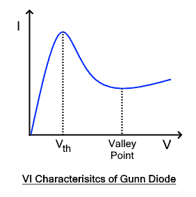
As evident from the graph, the current initially increases with an increase in the applied voltage up to the threshold voltage Vth. Once the voltage goes beyond Vth, the current starts to decrease as shown by the negative slope in the graph. This region is known as the negative resistance region. The Gunn diode is utilized in this region to generate high-frequency oscillation and also amplify the signals.
The current decreases down until the valley point. Further increase in the voltage increases the current again.
Related Posts:
- Schottky Diode: Construction, Working, Advantages and Applications
- Shockley Diode: Construction, Working, Characteristics and Applications
Gunn Diode Oscillator
Gunn diode is used to make an oscillator to generate microwave frequency in the range of 10 GHz to THz. Three negative resistance region of the Gunn diode is used for generating oscillation when very high voltage is applied to the Gunn diode known as the Gunn effect or transferred electron effect.
A DC bias voltage is applied to the Gunn diode which biases it into the negative resistance region. The negative differential resistance combines with the positive differential resistance of the circuit elements to cancel out each other and results in zero differential resistance. Therefore it generates sustained oscillation which can be controlled by the external circuit.
Advantages & Disadvantages
Advantages
Here are some advantages of Gunn diode:
- Gunn diode offers very high operating frequency in the hundreds of GHz range.
- It is a very economical and cheapest possible option for microwave frequency.
- It has small size and takes little space.
- It is very reliable in high-frequency operations.
- It is very comparatively very efficient.
- It has a large operating bandwidth.
- It has lower operating voltages.
- The signal-to-noise SNR value of the Gunn diode is very high as it is immune to noise.
Disadvantages
Here are some disadvantages of Gunn diode:
- The negative resistance region requires high voltage.
- Its efficiency deteriorates at a lower frequency below 10 GHz.
- The biasing temperature greatly affects its performance. Thus it has low stability.
- The noise immunity vanishes and the noise is high in certain applications.
Related Posts:
- Varactor Diode – Symbol, Construction, Working and Applications
- Constant Current Diode – Working, Construction, and Applications
Applications
Gunn diode is mainly used at microwave frequency.
- Gunn Oscillator: It is used in the Gunn oscillator to generate a very high frequency of 200 GHz. This oscillator is used in radio communication, microwave transmitter and receiver, and military radar.
- Oscillator and amplifier: the negative resistive region of the Gunn diode where the current and vintage vary inversely to each other is utilized to amplify a signal as well as oscillations.
- Sensor: it is also used in a sensor for the generation of microwave frequency such as in proximity detection systems, door opening systems, smart traffic signal controllers, security systems, intruder alarms, distance indicators, process control systems, level sensors, etc.
- Tachometer: Gunn diode is used in a contactless tachometer that is used for measuring the rotational speed of a wheel, motor shaft, etc. It sends a beam of microwave pulses that is reflected after each full rotation from the reflective mark. The speed is calculated in revolutions per minute RPM.
- Doppler Radar: it is used in continuous wave doppler radar to provide the velocity data of any object. It sends a microwave pulse that bounces back off the object and calculates the velocity using the variation in the frequency of the transmitted signal.
- Pulsed Gunn Diode generator: it is used to generate current pulsed in the microwave frequency range.
Related Posts:
- LED – Light Emitting Diode: Construction, Working, Types and Applications
- Photodiode: Types, Construction, Operation, Modes, Performance and Applications
- Backward Diode: Construction, Operation, Characteristics and Applications
- What is a Laser Diode? Construction, Working, Types and Applications
- What is Avalanche Diode? Construction, Working, Types and Applications
- Tunnel Diode: Construction, Working, Advantages, and Applications
- Zener Diode – Symbol, Construction, Circuit, Working and Applications
- Blocking Diode and Bypass Diodes in a Solar Panel Junction Box
- Diode Formulas and Equations – Zenner, Shockley and Rectifier
- Diode Symbols – Electronic and Electrical Symbols
- Applications of Diodes
-
 Difference Between Edge Triggering and Level Triggering
-
 Difference between Zener Diode and Avalanche Diode
-
 Difference Between Amplifier and Operational Amplifier
-
 Difference Between Static RAM & Dynamic RAM – SRAM vs DRAM
-
 Difference Between Digital Latch and Flip-Flop Circuits
-
 Difference Between Combinational and Sequential Logic Circuits