Main Difference Between Shockley and Schottky Diode
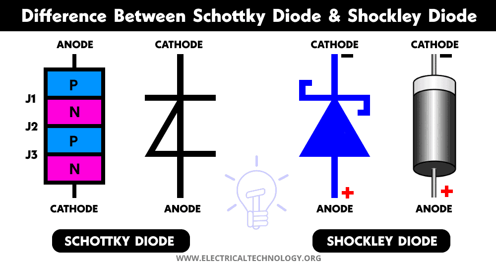
The diode is a semiconductor switch that allows current flow in only one direction. There are several types of diodes used in circuits for different applications. Schottky diode and Shockley diode both are two very different types of diodes. They should not be confused with each other as one of them is a metal-semiconductor junction diode while the other is a four-layer diode. Apart from this, there are several other differences between them.
Related Posts:
- Difference Between Schottky Diode and Fast Recovery Diode
- Difference Between Diode and SCR (Thyristor)
- Difference Between Diode and Transistor
Before going into the list of differences between the Schottky diode and the Shockley diode, let’s discuss their basics first.
Schottky Diode
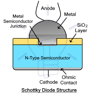
Schottky diode is a type of diode formed by a junction between metal and semiconductor. The junction is shortly known as the MS junction. It is also known as a hot carrier or Schottky barrier diode because only one type of the majority carriers is responsible for the current flow.
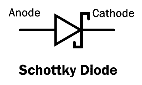
The MS junction allows a very low forward voltage drop with a very high switching speed due to the low capacitance between the metal and semiconductor junction. It is used in very high-frequency RF applications. The symbol of the Schottky diode is similar to a normal PN diode with the bar modified into an “S” shape.
Schottky diode is formed between N-type semiconductors and metals such as Aluminum, Platinum, tungsten, Chromium, gold, etc. The N-type layer is used instead of the P-type due to the high reverse leakage current. The forward voltage drop of the Schottky diode lies between 0.1 to 0.4 volts.
The width of the MS junction depends on the type of metal and the doping concentration of the semiconductor layer. This depletion layer determines the switching speed and voltage rating of the device. The low forward voltage drop makes it really efficient with very low power consumption.
The two terminals anode and cathode are internally connected with metal and semiconductor respectively.
- Related Post: Schottky Diode: Construction, Working and Applications
Shockley Diode
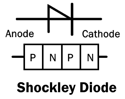
Shockley diode is a type of diode that is made of four alternating layers of semiconductor to form a PNPN structure. It is also known as PNPN or a four-layer diode. It is essentially a thyristor without the gate terminal. Since it has two terminals, it is classified as a diode. It has three PN junctions. Therefore, it conducts once the forward voltage exceeds the breakover voltage. The symbol of the Shockley diode resembles a half PN diode.
The structure of the Shockley diode resembles two PNP and NPN (BJT transistors) joined together. The base and collector of both BJTs are combined together. It also resembles three PN diodes connected in series where the second diode is in the reverse direction.
Shockley diode does conduct unless the voltage exceeds the breakover voltage. Until then it blocks the current conduction and the mode is called forward blocking mode. When it starts conduction, the voltage across the diode decreases while the current increase. The diode exhibits negative resistance therefore this region is known as the negative resistance region.
The Shockley diode cannot be easily switched as it is a latching device. To switch to off, the voltage across it must be reduced so that the current reduces below the holding current limit.
Shockley diode is not readily used and it is not commonly available in the market. however, it forms the backbone in the development of other semiconductor devices like DIAC, TRIAC and SCR, etc.
Key Differences between Schottky Diode & Shockley Diode
The following table shows the major differences and comparison between Shockley and Schottky Diodes.
| SCHOTTKY DIODE | SHOCKLEY DIODE |
| It was named after its inventor who was a German physicist named Walter H. Schottky. | It was invented by American physicist William Bradford Shockley hence the name. |
| It is a diode made from the metal-semiconductor junction. | It is a four-layer PNPN diode. |
| It is made from two layers of metal and semiconductor | It is made of four alternating layers of semiconductor. |
| It has only one MS junction. | It has three PN junctions. |
| It is unipolar, the current flow is only due to a single type of majority carriers. | The current flow is due to both types of majority carriers electrons and holes. |
| It starts conduction once the voltage exceeds the junction barrier potential. | It starts conduction once the forward voltage exceeds the breakover voltage. |
| It does not have a negative resistance region. | It has a negative resistance region. |
| It has a very low forward voltage drop of about 0.4 volts max. | It has a large forward voltage drop. |
| It has low reverse voltage ratings. | It can block high reverse voltage. |
| It has a very small junction capacitance. | It has large junction capacitance. |
| It has a very high switching speed. | It has a very low switching speed. |
| It has a fast recovery time (Similar to FR Diode). | It has a slow recovery time. |
Related Posts:
- Difference Between Microprocessor and Microcontroller
- Difference Between 8085 & 8086 Microprocessor – Comparison
Main Differences between Schottky and Shockley diodes
Definition
- Schottky diode is a type of diode that is formed by a junction between metal and semiconductor.
- Shockley diode is a type of diode that is made of four alternating layers of semiconductor to form PNPN.
Structure
- Schottky diode is a two-layer device made of metal and N-type semiconductor.
- Shockley diode is made of four alternating layers of P-type and N-type semiconductors.
Current flow
- Since the Schottky diode has only a single semiconductor layer, a single type of majority carriers of the semiconductor layer is responsible for current flow.
- Shockley diode has multiple PN junctions where the current flow is due to the flow of both majority carriers electrons and holes.
Junctions
- The Schottky diode has only one metal-semiconductor junction.
- Shockley diode has three PN junctions
Power Consumption
- The Schottky diode has a low forward voltage drop. Therefore it has very low power consumption.
- Shockley diode has a higher forward voltage drop. Therefore it has a higher power consumption
Switching Speed
- The Schottky diode has a very high switching speed due to its low junction capacitance. The junction capacitance is low due to the thin depletion region, thanks to the metal and semiconductor junction.
- Shockley diode has very slow switching speed as there are several PN junctions involved with increased switch ON time and switch off time.
Related Posts:
- Differences Between Encoder and Decoder?
- Difference Between CPU and GPU – Comparison
- Difference Between RAM and ROM – Comparison
- Difference Between JFET and MOSFET
- Difference Between D-MOSFET and E-MOSFET
- Difference Between BJT and FET Transistors
- Difference Between NPN and PNP Transistor
- Difference Between DIAC and TRIAC
- What is The Difference Between Transistor & Thyristor (SCR)?
- Difference Between Synchronous and Asynchronous Transmission
- Difference Between Serial and Parallel Communication
- Difference between LED and Photodiode
- Difference Between LED and LDR
- Difference Between Photodiode and Phototransistor
- Difference between Photodiode and Photoresistor (LDR)
- Differences between Active and Passive Filter
- Differences Between Encoder and Decoder?
- Difference Between Multiplexer (MUX) & Demultiplexer (DEMUX)
- Applications of Diodes


 Difference Between Edge Triggering and Level Triggering
 Difference between Zener Diode and Avalanche Diode
 Difference Between Amplifier and Operational Amplifier
 Difference Between Static RAM & Dynamic RAM – SRAM vs DRAM
 Difference Between Digital Latch and Flip-Flop Circuits
 Difference Between Combinational and Sequential Logic Circuits