What is a Zener Diode? Symbols, Circuit Diagram, Construction, Working and Applications
What is a Zener Diode?
A Zener diode is a type of PN junction diode that is designed to conduct in both forward and reverse directions. It has heavily doped regions and is mainly used to conduct current in the reverse direction. It starts conducting in the reverse direction when the reverse voltage exceeds a certain limit known as the reverse breakdown or Zener breakdown voltage.
Unlike an ordinary diode, a Zener diode can and specially designed to operate in the reverse breakdown region. The voltage across the device remains constant during the breakdown region while the current varies.
Symbol of Zener Diode
The symbol of Zener diode resembles an ordinary diode except for the change in a little bend at the edges of the vertical line to make a shape that resembles “Z” as shown in the given figure.
- Related Post: Different Types of Diodes Symbols
Construction of Zener Diode
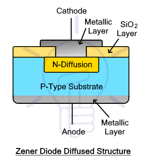
The Zener diode is constructed in a few different ways such as the diffused structure, diffused and passivated structure, and alloy diffused structure. Generally, we use the diffused structure of Zener diode whose figure is given below.
In this design, two N and P-type substrates are diffused together. On both sides, a metallic layer is used to form the cathode and anode terminals. Silicon oxide SiO2 layer is used to cover the junction regions and to prevent the contamination of the junction.
The structure of passivated Zener diode has its junction’s edges covered with a SiO2 layer. While the structure of alloy diffused Zener diode has all its junctions covered by SiO2 layer. The passivated structure offers better performance at higher voltage while the passivated structure offers better performance at lower voltages.
- Related Posts: What is Diode? Construction and Working of PN Junction Diode
Working of Zener Diode
The Zener diode can operate in both forward and reverse bias. In forward bias, it acts as a normal diode with nominal forward voltage drop and a large current flow. While in reverse bias, it blocks current flow until the applied voltage reaches the Zener breakdown voltage. This region is known as the Zener breakdown region and the Zener diode is specifically designed to operate in this region. The current starts to increase with an increase in the applied voltage while the voltage across the Zener remains the same.
The Zener voltage of the diode depends on the doping level which can be adjusted during the manufacturing of the Zener diode. The sudden increase in reverse current in a Zener diode is due to either one or both of the following effects.
Avalanche Breakdown or Effect
The avalanche breakdown can occur in both normal as well as Zener diode when the reverse voltage exceeds a certain limit. Due to the reverse voltage, the depletion region at the PN junction becomes wider and a potential difference generates across the depletion region. There is a small leakage current due to the flow of a small number of minority carriers through the junction. With an increase in the reverse voltage, the minority carrier gets enough energy to accelerate and starts to collide with the other atoms of the depletion region resulting in the release of free electrons. These free electrons collide with other atoms and release more free electrons which results in the flow of a huge current.
This mechanism is known as avalanche breakdown and it is destructive for normal diode as they cannot recover from this. But the Zener is constructed with proper doping levels to perform in this region. However, the avalanche breakdown does not provide a sharp voltage-current as does a Zener breakdown.
Zener Breakdown or Effect
The Zener breakdown occurs in the Zener diodes when a high reverse voltage is applied. Due to the heavy doping concentration, the depletion region has a narrow width. With an increase in the reverse voltage, the depletion region becomes wider forming a very strong electric field. Due to the high electric field, minority carriers accelerate and leaks through the depletion region and hits other atoms to release more electrons that take the form of a large reverse current.
The Zener breakdown is a safe method for Zener diode operation and it is specifically designed to operate in this region. The voltage across the Zener diode remains constant while the current increases. Therefore, this region is used for voltage regulation in many applications.
- Related Posts: Types of Diodes and Their Applications – 24 Types of Diodes
Circuit Diagram
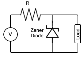
The following figure shows the circuit diagram for connecting a Zener diode which is connected in parallel to the load.
A voltage source is used whose voltage is higher than the Zener voltage of the diode. Whereas a resistor is used in series with the Zener diode and a load as a current limiting resistor to maintain the current.
The total current depends on the connected load. However, the voltage across the load remains constant i.e. the Zener voltage. This is why the Zener is used in various circuits to regulate the voltage.
Specifications of Zener Diode
The Zener diode is available with various specifications and they are used for different requirements. Therefore it is necessary to know the basic specs of a Zener diode.
- Zener Voltage
The Zener voltage Vz is the reverse breakdown voltage or the Zener breakdown voltage. It is the reference voltage that appears across the Zener diode in reverse biased. It can range from 2.4V to 200V.
- Current
The rated Zener current is the maximum current the diode can allow at the rated Zener voltage. It can range from 200 uA to 200A. The minimum current is the minimum current required for the breakdown that ranges between 5 mA to 10 mA.
- Power Rating
This is the maximum rated power the diode can tolerate. It is the product of Zener voltage and the current flowing through it. The power ratings of the Zener diode can range between 400 mW and 5 W.
- Voltage Tolerance
The voltage tolerance is the % difference that may occur in the said diode. Generally, the voltage tolerance of a Zener diode is +- 5%.
- Zener Resistance
The Zener resistance is the resistance of the diode in the ON state (Zener breakdown region). It is evident from the IV characteristic curve where the Curve is not completely vertical in the breakdown region.
IV Characteristics of Zener Diode
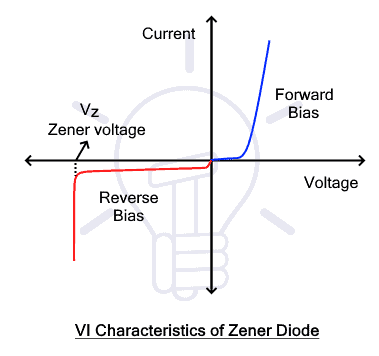
The IV characteristic curve shows the relation between the current and the voltage across the Zener diode. The given curve shows the operation of the Zener diode in both forward bias and reverse bias.
In forward bias, when the applied voltage is lower than the threshold voltage, the diode does not allow current through it but only the small leakage current. Once the applied voltage crosses the threshold limit, the current increases suddenly while the voltage remains constant. The forward bias operation in the Zener diode is the same as in any normal diode.
In reverse bias, the diode does not allow current (but only a small leakage current) until the voltage reaches the Zener breakdown voltage. In this region, the current through the diode flows in the reverse direction. The value of the Zener voltage is determined by the doping concentration in the diode.
Related Posts:
- Zener Diode and Zener Voltage Regulator Calculator
- Simple Overvoltage Protection Circuit using Zener Diode
Advantages and Disadvantages of Zener Diodes
Advantages
Here are some advantages of Zener diode
- Zener diode protects from voltage spikes and over-voltage.
- It is smaller in size.
- It can easily and efficiently stabilize the voltage.
- It can handle high voltages.
- It is cheaper and cost-effective.
Disadvantages
Here are some disadvantages of the Zener diode.
- It cannot handle a very large current.
- It provides a fixed output voltage that cannot be changed.
- The Zener current depends on the load current.
Applications of Zener Diode
The Zener diode is used in various applications. Here are some of the main applications of the Zener diode.
- As Voltage Regulator
A voltage regulator or stabilizer is a circuit that provides a stabilized and constant voltage even if the source voltage fluctuates or spikes. It removes or eliminates the fluctuations or voltage spikes that may damage the sensitive load connected to it.
A Zener is connected in parallel with the load to provide regulated voltage while a series resistor is used to maintain and limit the current flowing through the diode. The load voltage is the same as the Zener voltage VZ of the Zener diode.
- As Switch
Similar to a diode, its impedance changes with the level of the applied voltage. Due to such transition in impedance, it is used as a switch in certain devices.
- Clipper Circuit
A clipper circuit is an electronic circuit that is used to change the waveform or shape of a signal. It is done to protect certain sensitive components from over-voltage. A Zener diode is used in such circuits to clip off the peak of certain signals.
- Reference Signal
As the Zener provide a constant voltage, it is used as a reference signal for comparing voltage signal.
- Multimeter Protection
Multimeters are sensitive electronic devices that are often connected in the wrong configuration to high voltage or high current circuits. In such cases, a very high current flow through the meter can damage it. Therefore, a Zener diode connected in parallel is used to divert the excess current and protect the device from damage.
Related Posts:
- Applications of Diodes
- Diode Formulas and Equations – Zenner, Schockley and Rectifier
- How to Test a Diode using Digital and Analog Multimeter? – 4 Ways.
- Blocking Diode and Bypass Diodes in a Solar Panel Junction Box
- Simple Overvoltage Protection Circuit using Zener Diode
- PNP Transistor – Construction, Working and Applications
- NPN Transistor – Construction, Working and Applications
- Bipolar Junction Transistor (BJT) | Construction, Working, Types and Applications
- Thyristor and Silicon Controlled Rectifier (SCR) – Thyristors Applications
- Types of Transistors – BJT, FET, JFET, MOSFET, IGBT and Special Transistors
- MOSFET – Working, Types, Operation, Advantages, and Applications
- IGBT? Construction, Types, Working and Applications
- GTO? Types, Construction, Working and Applications
- DIAC? Symbol, Construction, Working and Applications
- TRIAC? Symbol, Construction, Working and Applications
- Difference Between Diode and SCR (Thyristor)
- Difference Between Diode and Transistor
- Difference Between Photodiode and Phototransistor


 Difference Between Edge Triggering and Level Triggering
 Difference between Zener Diode and Avalanche Diode
 Difference Between Amplifier and Operational Amplifier
 Difference Between Static RAM & Dynamic RAM – SRAM vs DRAM
 Difference Between Digital Latch and Flip-Flop Circuits
 Difference Between Combinational and Sequential Logic Circuits